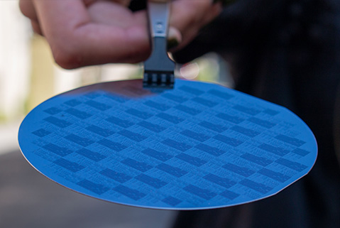
Semiconductor fabrication
UCLA AND HUGHES RESEARCH LAB
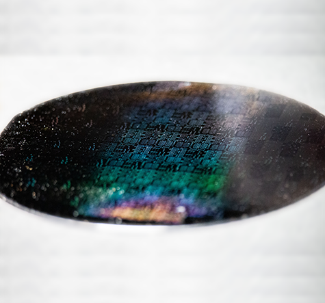
Photo of a wafer exposure that I personally personally fabricated at the UCLA Nanofabrication Labratory. It serves as an excellent visual aid for Nanofabrication concepts.
With dedication to expanding my understanding of technological innovation, I applied to UCLA's Nanofabrication Laboratory for a Summer 2024 Research Internship opportunity. After early training, this opportunity bridged into a full-time internship at Hughes Research Laboratory (HRL) in Malibu, California, which exposed me to advanced microfabrication systems and projects.
At HRL, I was exposed to the many areas of the facility and gathered skills in my concentration of photolithography and a broader exposure to various other labratories of the company. This opportunity provided experience to work in a facility that dances between commercial collaboration and advanced research. Ultimately, this opportunity left me excited to continue my journey in refining my engineering skillsets into the future.
Experiences
UCLA NANOFABRICATION LABRATORY
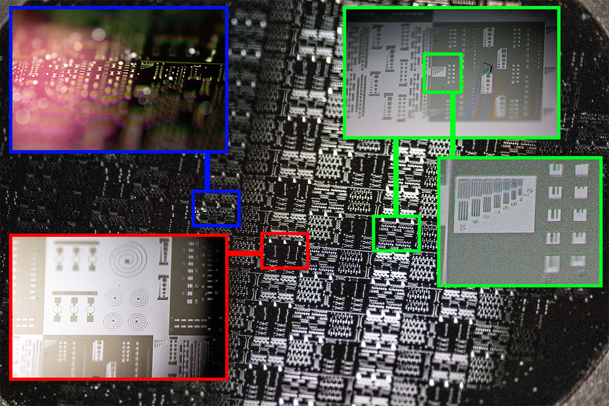
My application to UCLA's Summer program resulted in training in both classical photolithography techniques as well as modern processes involving electron beam lithography. I was exposed to the first principles of lithography and nanofabrication concepts, and this ultimately taught me foundations in the engineering lifecycle of designing, fabricating, qualifying, and sustaining chips and wafers. Ultimately, I was emersed in hands-on learning related to the field of semiconductor manufacturing and nano-scale processes. I operated with chip mask alignment, coat procedures, electron beam lithography, and chemical vapor deposition systems. It was an amazing experience to have exposure to such an innovative area of engineering at a top research institution.
hughes research labratory (hrl)
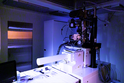
At HRL, the opportunity to learn is endless. After taking in the many beautiful views of Malibu, California, I dove into intern projects associated with positively impacting the Microfabrication Technology Laboratory (MTL). In HRL, I created and optimized recipes for novel photoresists in semiconductor manufacturing, focusing on coating, developing, exposing, and patterning wafers. Additionally, I addressed challenges in resist uniformity during wafer coating. I worked to improve measurement precision during the development process by designing trials to test wafer spin speed, spin time, and bake temperature to solve uniformity issues.
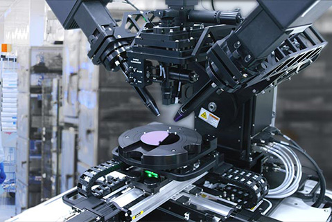
Related to equipment, I gained proficiency in using Canon steppers, Nikon metrology, reflectometry tools, electron microscopes, and statistical analysis for validating repeatability and functionality of wafer processing. Each of these skills has wide-ranging applications in a variety of engineering fields.
First Principles Understanding
Through both UCLA and HRL opportunities, I learned the valuable lesson that having a detailed understanding of any given engineering system is crucial before making changes and modifications. This avoids regression or negative impact within a production environment. Applying first principles engineering thinking is also key: breaking down a problem into it's fundimental truths to determine how to solve it most effectively. With such a mindset, engineering solutions present themselves and my personal intuition improves.
